- +1
We have 18k+ Customers word-wide


STEP 01
IT Support
Delivering innovative solutions for oil and gas exploration, production, and refining, with a focus on efficiency and safety.

Step 02
Cyber Security
Delivering innovative solutions for oil and gas exploration, production, and refining, with a focus on efficiency and safety.

Step 03
IT Consultant
Delivering innovative solutions for oil and gas exploration, production, and refining, with a focus on efficiency and safety.

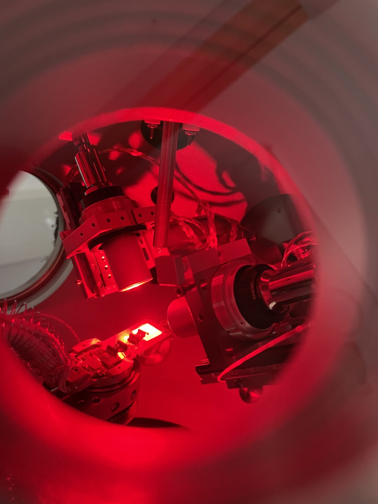
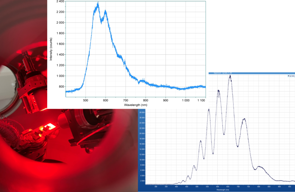
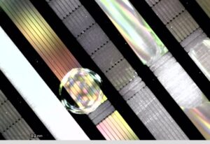
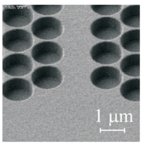
01 - gallium nitride
Cathodo-luminescence
GaN exhibits intense broadband emission by bombardment by an electron beam. The spectra here demonstrate CL from MOCVD-GaN/Saphire obtained in HV 10^-7 mbar under Excitation by e-gun 3 kV with Grating monochromator 600 gr/mm, TEC CCD.
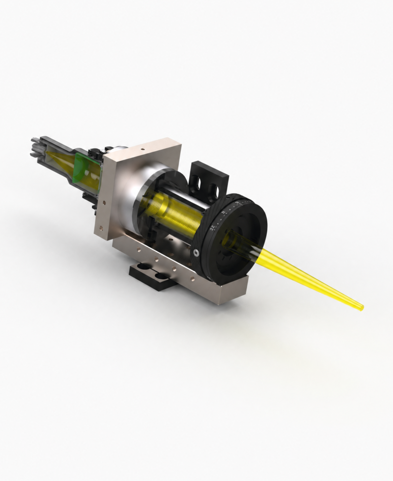
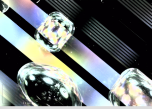
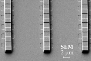
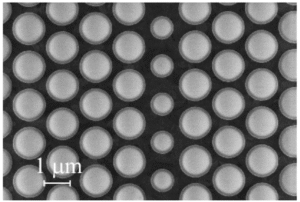
02 - meta-materials
Diffraction and Reflection
Fishnet structure has
1. Negative refractive index (n < 0) - The coupled plasmonic currents in the layered “fishnet” structure generate simultaneously negative permittivity and permeability, producing a negative index of refraction.
2. Optical-frequency operation - the structures demonstrate negative index in NIR/VIS regime, enabled by plasmonic coupling between the patterned metal layers.

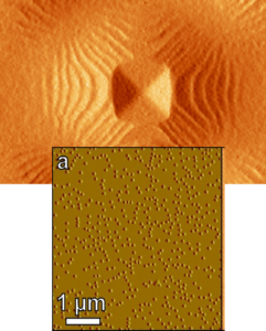
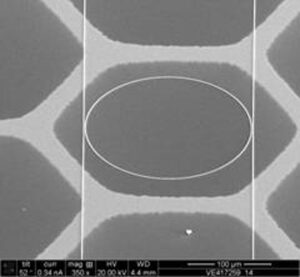
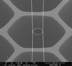
03
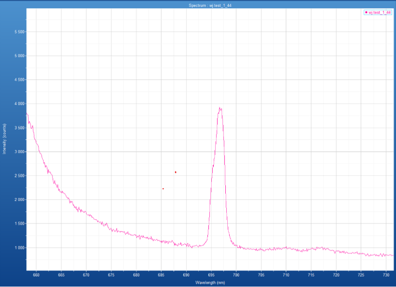
Raman spectroscopy
Raman mapping of SiC can identify polytype inclusions, strain and defect types (e.g. micropipes cause local peak shifts/intensity changes).


Demon Cats
President

Simmy Flavius
Vice president

Emily Carter
Consultant

Simon Cyrene
Manager

Paul Flavius
Coordinator

Mellissa Doe
Analyst

Kevin Lee
IT Support

Anne Smith
Officer
Demon Cats
President
Simmy Flavius
Vice president
Emily Carter
Consultant
Simon Cyrene
Manager
Paul Flavius
Coordinator
Mellissa Doe
Analyst
Kevin Lee
IT Support
Anne Smith
Officer